AEC Q100-011-Rev-C1-2013 (CDM), AEC Q100-002-Rev-E-2013 (HBM) and AEC Q100-004D-2012 (Latch-Up) are automotive ESD stress procedures. ANSI/ESDA/JEDEC JS-002-2014 (CDM), ANSI/ESDA/JEDEC JS-001-2017 (HBM), and JESD78E-2016 (Latch Up) are non-automotive ESD stress procedures. MM (Machine Model) is no longer a supported ESD stress simulation model for both automotive and non automotive. Automotive System ESD (ISO 10605:2008) is a modification to stress procedures found in System ESD (IEC 61000-4-2:2008). The following table will explain the differences between non-automotive and automotive ESD stress Procedures:
Comparison of Non-Automotive and Automotive ESD Stress Procedures
| Stress Type | Non-Automotive | Automotive |
|---|---|---|
| HBM | ANSI/ESDA/JEDEC JS-001-2017 | AEC Q100-002-Rev-E-2013 |
| HBM Note1 | Stress Levels: +/-1000v | Stress Levels: +/-500v, +/-1000v, +/-2000v |
| HBM | Use single stress + polarity for power supplies to minimize tester parasitics | Use legacy stress pin combinations, unless tester artifacts are proven to cause false failures |
| HBM Note2 | Use symmetric + supply to individual non-supply stress for - non-supply to supply stress | Use +/- stresses for all combination unless tester artifacts are proven to cause false failures |
| HBM | Only one pin of a group of supply pins connected to a common plane needs to be stressed | All supply pins need to be stressed |
| CDM | ANSI/ESDA/JEDEC JS-002-2014 | AEC Q100-011-Rev-C1-2013 |
| CDM | Each pin is required to be stressed once with +/- stress pulse | Each pin is required to be stressed three times with +/- stress pulse |
| CDM | Corner package pins are not required to be stressed at a higher CDM voltage compared to other package pins | Corner package pins are required to be stressed at +/-750v |
| CDM Note3 | AEC CDM stress can realize 60% higher pin discharge current compared to JS stress at same voltage using same package and discharging same pin. | |
| CDM Note4 | Pin stress voltages of +/-250v | Pin stress voltages of +/-250v, +/-500v for non-corner package pins, and +/-750v for package corner pins. |
| Latch-UP Note5 | JESD78E 2016 | AEC-Q100-004D 2012 |
| Latch-UP | Maximum ambient temperature for stress 85 degrC | Maximum ambient temperature for stress test is 125 degrC |
| System ESD | IEC 61000-4-2:2008 | ISO 10605:2008 |
| System ESD | +/-8kv for contact and air gap discharge stress level and +/-15kv airgap discharge stress level only | +/-4kv, +/-6kv, and +/-8kv for contact and air gap stress level and +/-15kv and +/-25kv for air gap discharge stress only |
| System ESD Note6 | 150pf/330 Ohms stress gun charge module | 150pf/2000 Ohms stress module for components located in the trunk, 330pf/2000 Ohms stress module for components located in the passenger compartment |
| System ESD Note7 | Only stress pcb connector shields, remote cabling stress not required | Stress conductor and ground shield at end of 1.7m remote communication cable |
| System ESD | Only stress when system is powered on | Stress when system is powered on and off |
| System ESD | Stress gun is referenced to ground plane on which stress table resides | Stress gun is referenced to stress table top ground plane |
HBM Note1: For Ansi/ESDA/JEDEC JS001-2017, industry consortium recommends an integrated circuit pass HBM pin stress at +/-1000v. Passing this level of stress simulation in conjunction with appropriate integrated circuit handling procedures in a typical manufacturing environment allows this integrated circuit to contain sufficient ESD robustness.
HBM Note2: For Ansi/ESDA/JEDEC JS001-2017 specialstress procedures are allowed to overcome HBM stress tester pulse slew rate issues due to stress tester parasitic capacitance. These tester parasitics are also known as stress tester artifacts and cumulative stresses.
CDM Note3: The difference is due a different charge plate used by Q100 CDM stress simulators vs JS CDM stress simulators.
CDM Note4: For Ansi/ESDA/JEDEC JS002-2014, industry consortium recommends an integrated circuit pass CDM pin stress at +/-250v. Passing this level of stress simulation in conjunction with appropriate integrated circuit handling procedures in a typical manufacturing environment allows this integrated circuit to contain sufficient ESD robustness.
Latch-Up Note5: For JESD78E 2016 and AEC-Q100-004D 2012 stress test procedures for Latch Up simulation are the same except where noted in the table.
System ESD Note6: ISO 10605:2008 describes vehicle specific requirements for System ESD stress except for pyrotechnic modules (air bags).
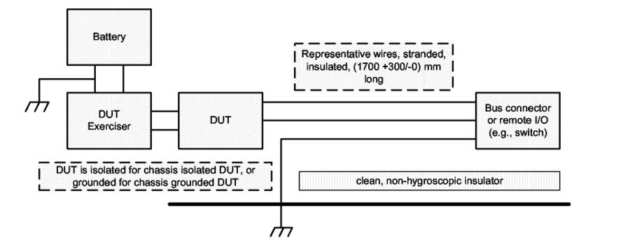
System ESD Note7: ISO 10605:2008 special stress simulation set up for remote inputs/outputs as shown in picture below:
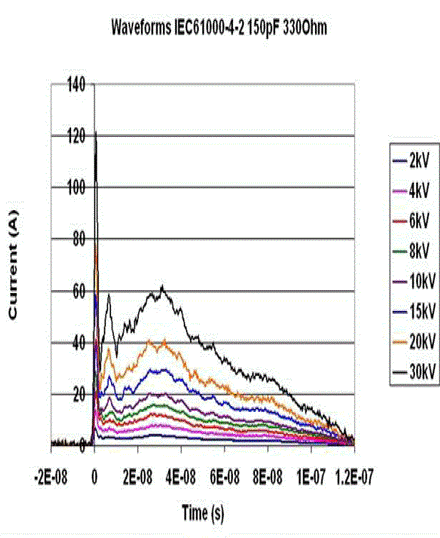
Below stress waveforms are for IEC stresses:
Link to other ESD and Latch-Up topics:
- Human Body Model (HBM) Charged Device Model (CDM) Machine Model (MM) System Level ESD - IEC 61000-4-2 Electrical Fast Transients(EFT)/Burst - IEC 61000-4-4 Lightning/Surge - IEC 61000-4-5 Latch-Up Electrical Overstress (EOS) ESD and Latch Up Testing and Qualification Procedures
For immediate consulting help on the above topics, contact Visitors Since June 16, 2019:
Current local date and time in Alpine, Texas (United States)