Electro Static Overstress (EOS) Details
Some Causes of Electro Static Overstress (EOS) |
|---|
| Power supply voltage surges above its absolute maximum rating (AMR) . |
| Signals on pcb may have high voltage transients which are above IC's AMR. |
| External to pcb switching inductive or capacitive loads can induce high voltage transients which are above IC's AMR. |
| Excessive noise on pcb ground plane due to switching IO's over/undershoots inducing high voltage transients which are above IC's AMR . |
| Exessive pcb signal noise induced by EMI (electromagnetic interference) causing high voltage transients which are above IC's AMR. |
| Hot socketing or misalignment of IC into powered up pcb causing high voltage transients at IC's pins which are above IC's AMR. |
| Uncontrolled Latch-Up event at IC's pins causing extreme high currents to flow for an extended time. |
| Floating IC pins picking up system noise which is above IC's pin AMR. |
| Improper IC power supply sequencing causing uncontrolled Latch-Up even in an IC. |
| Poorly grounded operators handling IC's. |
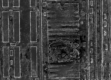
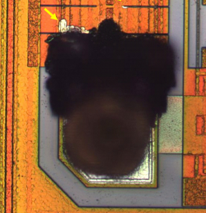
The below images are examples of silicon damage as a result of EOS. The image on the below left shows catastrophic damage at the silicon level in a pad connected transistor, while the image on the right shows precipiation of die encapsulation material at a device pin due to extremely high temperatures during an EOS event at the device pin.
For immediate consulting help on the above topics, contact (blog with) the ESD Unlimited LLC staff at the
Links to other ESD and Latch Up topics
- Charged Device Model (CDM) Machine Model (MM) System Level ESD - IEC 61000-4-2 Electrical Fast Transients (EFT)/Burst - IEC 61000-4-4 Lightning/Surge - IEC 61000-4-5 Automotive ESD - AEC Q100 and ISO 10605 Latch-Up ESD and Latch Up Testing and Qualification Procedures
Current local date and time in Alpine, Texas (United States)
Visitors Since June 16, 2019: