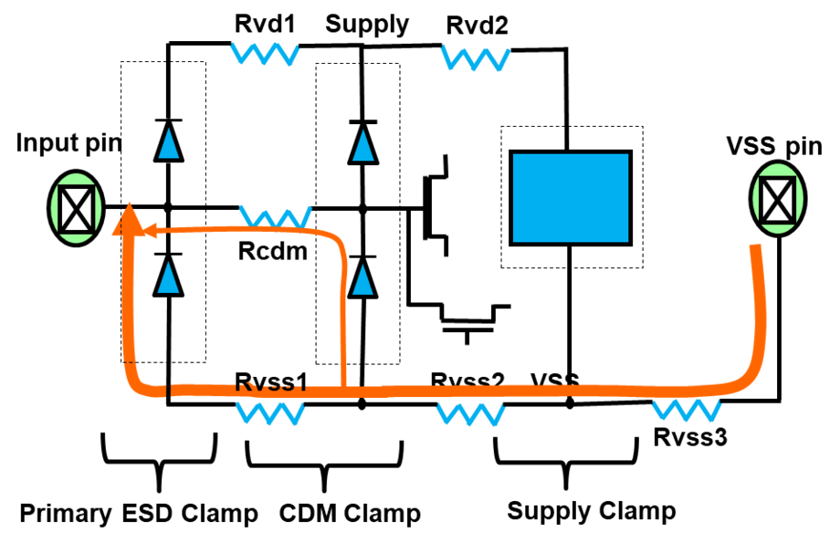
The Charged Device Model (CDM) is the ESD model which best simulates real time integrated circuit ESD threats. For example, this model covers the situation when an integrated circuit component package builds up a charge traveling through an integrated circuit automatic handler system and the integrated circuit pin comes into contact with the grounded surface of the automatic handler and discharges the built up package charge through a single pin coming in contact with a grounded surface. This is shown in the below schematic and described by the equivalent circuit.

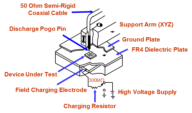
The picture in the below left is a hardware drawing of a typical CDM stress simulator. The integrated circuit is placed in a "dead bug" position on the stress platform and charged up to the stress specification voltage. The CDM stress simulator then touches a pogo pin on one of the integrated circuit package pins and discharges the package charge through this pin. Thermo Fisher Scientific, and Electro-Tech Systems are a few of the CDM stress simulator manufacturers used in the industry. The picture in the below right shows a electrical schematic of the CDM stress simulator.

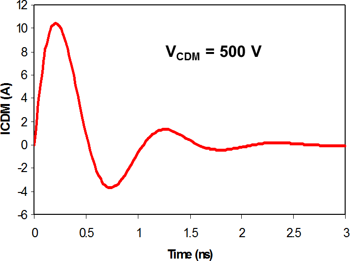
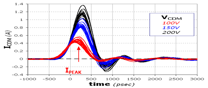
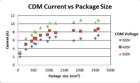
The picture in the below left illustrates the CDM discharge current flowing in an integrated circuit pin after an integrated circuit package is charged with 500v CDM stress voltage. The picture in the below right illustrates that for the same package size, the higher the pre-charge voltage of the integrated circuit package the higher the discharge current flowing in the package pin being discharged. The picture in the below center illustrates how integrated circuit package capacitance increases with size of the package which means that integrated circuit CDM pin discharge currents increase as their package sizes increase.
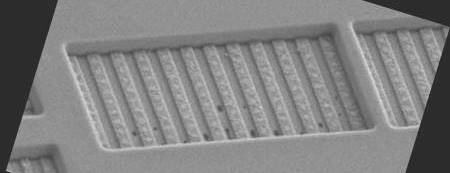
The below picture on the left represents positive CDM stress of an input pin, The orange path indicates the current discharge path for this pin during stress. The below picture on the right shows thin oxide gate damage to the gate oxide area at the drain of an output transistor after 500v (10A) CDM stress at the pin.
For further information on CDM stress procedures see:
How To Solve CDM ESD Failures
CDM ESD failures are a caused when the voltage buildup on the gate of a transistor during CDM ESD stress exceeds the damage voltage of the gate's thin oxide and causes the gate oxide to rupture.
How the CDM ESD Stress is Applied to the Integrated Circuit Pins
The CDM stress is applied to the pins of an integrated circuit in a two step process. First, the integrated circuit package is placed in a "dead bug" position on a stress simulator charge plate and the integrated circuit package is charged up to a specified voltage (anywhere from 100v to 750v). Second, each pin of the integrated circuit is discharged one after another after successive integrated circuit package charge cycles. This means that during the CDM simulation, each pin of an integrated circuit discharges the current developed from the integrated circuit package charge cycle.
Key Factors in Understanding CDM ESD failures
1: The currents flowing through an integrated circuit package pin are in the range of 1A to 15A depending on the size of the integrated circuit package and the magnitude of the integrated circuits package charge voltage during the CDM simulation. As can be seen from the above circuit schematic, the lower the resistance of the ESD protection diodes, supply leads, and supply clamp during the pin CDM discharge event, the lower the voltage build up on the integrated circuit pin.
2: Weather is is a positive CDM stress or a negative CDM stress, keeping the voltage build up on the stressed integrated circuit pin below the thin oxide damage voltage is the key to solving CDM ESD damage failures.
3: More information about CDM stress voltages and CDM stress procedures is given at:
Links to other ESD and Latch Up topics
- Human Body Model (HBM) Machine Model (MM) System Level ESD - IEC 61000-4-2 Electrical Fast Transients (EFT)/Burst - IEC 61000-4-4 Lightning/Surge - IEC 61000-4-5 Automotive ESD - AEC Q100 and ISO 10605 Latch-Up Electrical Overstress (EOS) ESD and Latch Up Testing and Qualification Procedures
For immediate consulting help on the above topics, contact (blog with) ESD Unlimited LLC staff at the
Current local date and time in Alpine, Texas (United States)
Visitors Since June 16, 2019: