The Human Body Model (HBM) is the most commonly used model for characterizing the susceptibility of an electronic device to damages from electrostatic discharges (ESD). The model simulates the discharge of a person's built up charge into the pins of a grounded integrated circuit component. This charge can be acquired by the person when walking across carpet, vinyl floor or other means. The below schematic shows the process of a person discharging their built up charge into the pins of an integrated circuit and the resulting schematic of this event.

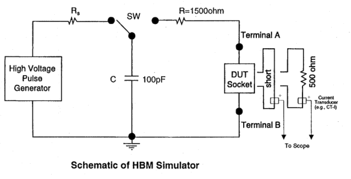
The below picture is a electrical schematic of a typical HBM stress simulator. Many industry stress labs use HBM stress simulators similar to the Keytek division of Thermo Scientific Mk.4 or NoiseKen ESS-6002 component level Electrostatic Discharge Simulator.
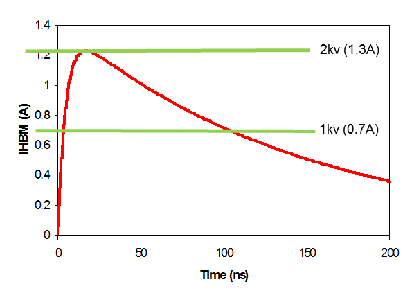
The below picture shows the HBM stress waveform applied to the integrated circuits pins during the HBM simulation. The graph indicates the expected currents at the integrated circuit pins under stress for a 1kv and a 2kv HBM stress pulse.
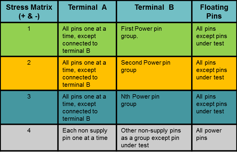
The HBM integrated circuit stress procedure divides the integrated circuits pins into Power and all other pins and designates pin groupings to the stress testers Terminal A (applied stress terminal), and Terminal B (reference terminal). Each pin of the integrated circuit is stressed with a positive and a negative stress pulse. An example of the pin stress combinations during an HBM stress test is given in the figure below. Further details on the HBM stress procedures can be found at below link:
ESD and Latch Up Testing and Qualification
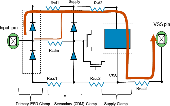
The below picture is a representation of a positive Input pin to VSS HBM stress of a typical integrated circuit digital Input buffer. Terminal A (the applied stress terminal) of the stress tester is connected to the Input pad and Terminal B (the reference stress terminal) of the stress tester is connected to the VSS or reference pad. The ESD portion of the Input buffer consists of an Input pad, a Primary ESD Clamp, a Secondary ESD Clamp, a ESD Supply Clamp and parasitic resistances (Rvd1, Rvd2, Rvss1, Rvss2, and Rvss3) connecting these ESD protection components.
The orange trace indicates the direction of ESD stress current during a positive Input pin to VSS pin stress. The goal of the ESD structures is to clamp the voltage at the Input pad to be lower than the damage voltage of the input transistor oxide (depending on process this could be between ~5v-9v). As can be seen from the schematic, the values of the Primary ESD Clamp Diode resistances, supply resistances (Rvd1, Rvd2), the VSS resistance (Rvss1, Rvss2, Rvss3), and the turn on characteristic of the Supply Clamp play important roles in keeping the Input pad voltage below the damage voltage level of the input thin oxide transistor during a positive HBM stress.
The below scanning electron microscope picture shows the damage to a input transistor thin oxide of a typical digital integrated circuit Input buffer. In this case, the input pad voltage during a 2kv Input pin to VSS stress exceeded the damage voltage level on the gate oxide. In the below picture, the dark areas are the gate oxide and the gray areas are the source/drain regions of the transistor.

How To Solve HBM ESD Failures
HBM ESD failures are a caused when the the voltage buildup on the gate of a transistor during HBM ESD stress exceeds the damage voltage of the gate's thin oxide and causes the gate oxide to rupture. Damage to contact structures or other integrated circuit topology in the path of the ESD current are also possible.
The HBM stress is applied between two pins of the integrated circuit. A positive/negative stress pulse is applied to the designated positive/negative pin and referenced to a designated negative/positive pin of an integrated circuit, this stress pulse forces positive/negative stress current to flow from the designated positive/negative to the designated negative/positive pin of the integrated circuit. (see above stress current flow schematic for positive stress current).
Key Factors in Understanding HBM ESD failures
1: The lower the resistance values of the ESD protection diodes, supply and vss interconnect resistances, and the supply clamp in the stress current path, the lower the voltage build up on the integrated circuit pin during a positive or negative applied HBM stress to an integrated circuits pin.
2: Weather is is a positive HBM stress or a negative HBM stress, keeping the voltage build up on the stressed integrated circuit pin below the thin oxide or topology damage voltage is the key to solving HBM ESD damage failures.
3: More information about HBM stress voltages and HBM stress procedures is given at:
Links to other ESD and Latch Up topics
- Charged Device Model (CDM) Machine Model (MM) System Level ESD - IEC 61000-4-2 Electrical Fast Transients (EFT)/Burst - IEC 61000-4-4 Lightning/Surge - IEC 61000-4-5 Automotive ESD - AEC Q100 and ISO 10605 Latch-Up Electrical Overstress (EOS) ESD and Latch Up Testing and Qualification Procedures
For immediate consulting help on the above topics, contact (blog with) ESD Unlimited LLC staff at the
Current local date and time in Alpine, Texas (United States)
Visitors Since June 16, 2019: