
What is Voltage Induced Latch-Up?
Voltage induced Latch-Up is a failure of an integrated circuit in which one or more low impedance paths is created between an integrated circuits power supply and its ground rails. This low impedance condition continues to be present after removal of a trigger condition that arises from:
1: Applying greater (or less than) than the maximum (minimum) specified voltage to an integrated circuit pin.
2: Causing the input voltage of an IO pin to rise above its power rail (or below its ground rail) by a diode drop or greater without limiting input current.
3: Not managing the ramp sequence of multiple distinct integrated circuit power supplies which may cause input voltages of internal stages to be a diode drop or more higher than their interacting power supply.
4: Uncontrolled +/- voltage noise on I/O pins of an integrated circuit causing the input voltage of I/O pins to be a diode drop or more higher (lower) than their interacting power supply (or ground domain).
What is Signal Latch-Up?
Signal Latch-Up is a failure of an integrated circuit in which one or more low impedance paths is created between one of the integrated circuits signal pins and its associated ground domain. This low impedance path continues to be present even after removal of a trigger condition that arises from:
1: Causing the input voltage (when set to a logical "HI") of an IO pin to rise above its power rail by a diode drop or more without limiting input current.
2: Causing the input voltage (when set to a logical "LO") of an IO pin to fall below its ground rail by a diode drop or more without limiting input current.
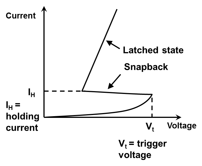
Graphical Explanation of Latch-Up
The below picture is the current waveform of a Latch-Up event. As soon as the parasitic thyristor latching circuit has triggered (Vt= trigger voltage) snapback occurs and the integrated circuit is latched. At this point extremely high currents (Amps) will flow between the integrated circuits Supply Rail and Ground Rail through turned on thyristor (see further below picture on the right). If this current is not limited (clamped), the integrated circuit will eventually destruct.
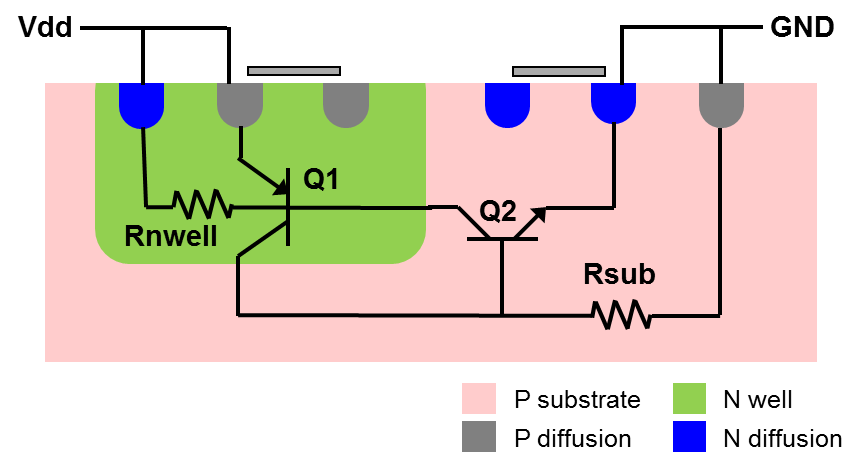
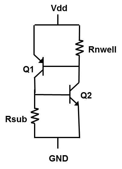
The below pictures show a topological (on the left) and a transistor schematic (on the right) describing the Latch-Up thyristor configuration. As can be seen, Latch-Up occurs when parasitic transistors Q1 and Q2 turn on and provides a self sustaining low impedance path between the power and ground rails.
How to Avoid Latch-Up
1: In the integrated circuit topology, surround all current injection points with guard rings.
2: In the Integrated circuit topology, reduce parasitic circuit Rsub, Rnwell and reduce gain of parasitic transistors Q1 and Q2 (see above figure on the left).
3. Avoid positive and negative pcb trace noise at the integrated circuit signal pins of one diode drop or more above and below the power and ground rails.
4: Insure Power supply ramp sequence of multiple power supplies of an integrated circuit do not cause internal input stages to be of greater voltage that their interacting supplies.
More information about Latch-Up Robustness Stress Testing and Qualification is at:
Link to other ESD and Latch-Up topics:
- Human Body Model (HBM) Charged Device Model (CDM) Machine Model (MM) System Level ESD - IEC 61000-4-2 Electrical Fast Transients(EFT)/Burst - IEC 61000-4-4 Lightning/Surge - IEC 61000-4-5 Automotive ESD - AEC Q100 and ISO 10605 Electrical Overstress (EOS) ESD and Latch Up Testing and Qualification Procedures
For immediate consulting help on the above topics, contact (blog with) ESD Unlimited LLC staff at the
Current local date and time in Alpine, Texas (United States)
Visitors Since June 16, 2019: