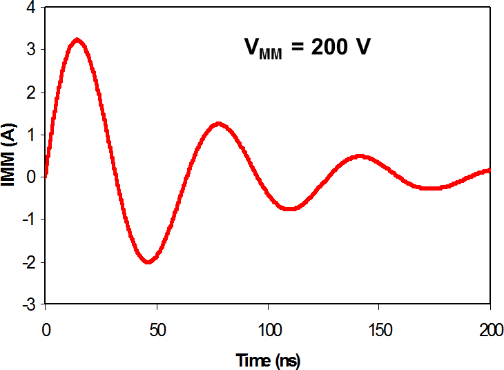
The Machine Model (MM) is the ESD model which is intended to simulate abrupt discharge events which are caused by contact with equipment and empty sockets (functional test, burn in, reliability testing, etc.). The model was developed in Japan and is widely used there. The model is very sensitive to parasitics and control of testers and to comply with standards is very difficult. The MM model stress current levels are much higher than the stress current levels for the HBM model. For a 200 V MM stress levels the peak current is 3.5 Amps or a equivqlent 4kv HBM ESD stress pulse. Unless specifically required by customers, MM stress is for information only. The MM model has been replaced by more accurate CDM and HBM models.
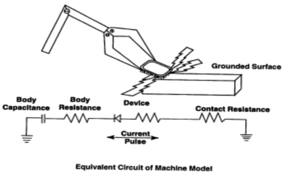
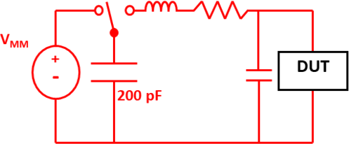
The picture below left is an equivalent circuit of the MM simulator and the picture on the right is the current stress waveform of a 200v MM model stress pulse.
For further information on the MM stress procedures see:
How To Solve MM ESD Failures
MM ESD failures are a caused when the the voltage buildup on the gate (or source/drain) of a transistor during MM ESD stress exceeds the damage voltage of the gate's thin oxide and causes the gate oxide to rupture.
How the MM ESD Stress is Applied to the Integrated Circuit Pins
The MM stress is applied between two pins of the integrated circuit. A positive/negative stress pulse is applied to the designated positive/negative pin and referenced to a designated negative/positive pin, this stress pulse forces positive/negative stress current to flow from the designated positive/negative pin to the designated negative/positive pin of the integrated circuit. (see stress current flow schematic on the HBM page of this website).
Key Factors in Understanding MM ESD failures
1: The lower the resistance values of the ESD diodes, interconnect resistances, and supply clamp is in the stress current path, the lower the voltage build up on the integrated circuit pin where the positive/negative stress is applied.
2: Weather is is a positive MM stress or a negative MM stress, keeping the voltage build up on the stressed integrated circuit pin below the thin oxide damage voltage is the key to solving MM ESD damage failures.
4: A few OEM's require qualification with MM stress, these are Japanese, Automotive, and several domestic manufacturers. It is known that 200v MM develops the same stress current as 4kv HBM, as a result, several domestic OEM's have lowered their MM voltage requirements.
3: More information about MM stress voltages and MM stress procedures is given at:
Links to other ESD and Latch Up topics
- Human Body Model (HBM) Charged Device Model (CDM) System Level ESD - IEC 61000-4-2 Electrical Fast Transients (EFT)/Burst - IEC 61000-4-4 Lightning/Surge - IEC 61000-4-5 Automotive ESD - AEC Q100 and ISO 10605 Latch-Up Electrical Overstress (EOS) ESD and Latch Up Testing and Qualification Procedures
For immediate consulting help on the above topics, contact (blog with) ESD Unlimited LLC staff at the
Current local date and time in Alpine, Texas (United States)
Visitors Since June 16, 2019: